Delegates attending the Fall Meeting of the Materials Research Society will be able to explore the latest products and services for preparing, analysing and studying novel materials and devices
Thousands of scientists and engineers will be converging in Boston at the end of November for the Fall Meeting of the Materials Research Society, the largest international scientific gathering for materials research. More than 50 technical symposia during the event will showcase leading interdisciplinary research in both fundamental and applied areas, presented by scientists from all over the world.
This year’s conference maintains the hybrid approach introduced in 2021, with the live meeting kicking off at the Hynes Convention Center in Boston on 27 November. A dedicated virtual event will run on 6–8 December, with online delegates also able to tune into live streams of featured talks during the in-person event.
This year also sees the return of the iMatSci Innovation Showcase, which provides a platform for scientists and engineers to demonstrate the practical applications of materials-based technologies. iMatSci aims to connect these innovators with early-stage investors, corporate technology leaders and potential partners, fostering collaborations that will accelerate the adoption of new materials technologies for real-world applications.
Alongside the wide-ranging programme of technical presentations, tutorials and professional-development sessions, the technical exhibit offers delegates the opportunity to connect with more than 150 companies showcasing the latest innovations for advancing materials research. A few of the highlights are detailed below.
Probe insert offers integrated solution for Hall analysis
In addition to reducing the time needed to perform Hall effect measurements, Lake Shore’s MeasureReady M91-HR FastHall measurement controller can be used with any type of magnet, including superconducting devices. One such magnet system is the Physical Property Measurement System (PPMS) from Quantum Design, which through a new probe insert from Lake Shore can now be easily integrated with the M91-HR. A specialized version of the insert enables high-resistance measurements up to 200 GΩ, while a standard kit for measurements between 10 mΩ and 10 MΩ is also available.
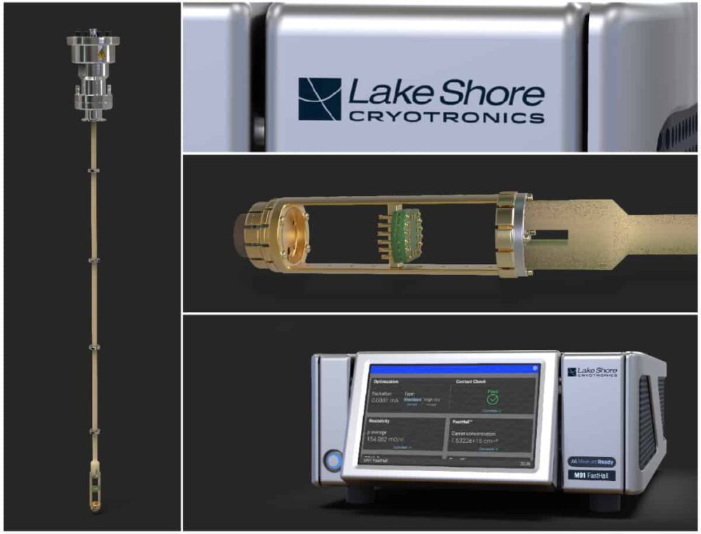
The new insert works with both van der Pauw and Hall bar geometries, with samples wired to specially designed sample boards. Fully guarded connections from the PPMS-inserted probe to the M91 instrument ensure ultralow noise measurements. The solution is simple to implement, with the M91-HR’s control software integrating easily with the MultiVu system installed on the PPMS. Preloaded scripts enable complete Hall measurement sequences to be executed quickly within the PPMS environment.
The M91-HR combines all necessary Hall measurement functions into a single instrument, automating the measurement process and directly reporting the calculated parameters. Its speed of measurements results from Lake Shore’s patented FastHall technique, which fundamentally changes the way the Hall effect is measured by eliminating the need to switch the polarity of the applied magnetic field during a measurement. This results in faster, more precise measurements, allowing the analysis time in some cases to be reduced by a factor of 100. Most commonly measured materials can be analysed in a few seconds, and even low-mobility (down to approximately 0.001 cm2/V s) samples can generally be measured.
- Visit Lake Shore Cryotronics at booth #908
Correlative microscope combines AFM and SEM capabilities
Quantum Design has released the FusionScope, an innovative correlative microscope that combines the measurement power of AFM with the benefits of SEM imaging. Designed from the ground up to seamlessly integrate these two powerful techniques, the FusionScope exploits a shared co-ordinate system that automatically aligns both AFM and SEM operations. This shared mapping system makes it quick and easy to identify the area of interest, measure the sample, and combine the imaging data in real time.
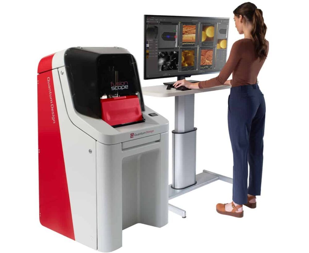
“The ability to scan and image across differing magnification scales in the FusionScope is the system’s major enabling attribute,” said Stefano Spagna, the company’s chief technology officer. “It allows smooth image transitions between millimetre, micron, and sub-nanometre scales, allowing you to see new correspondences in your data from specific sample areas.”
FusionScope supports most standard AFM measurement modes. It also offers the Finite Impulse Response Excitation (FIRE) mode, a novel off-resonance intermittent contact scanning force microscopy technique that characterizes nanomechanical properties such as sample stiffness and tip adhesion. Advanced AFM techniques include conductive atomic force microscopy and magnetic force microscopy, and switching to these specialized measurement modes can be achieved simply by swapping the self-sensing cantilevers available with the system.
The software provided with the FusionScope can be used to interactively overlay AFM imaging data onto SEM images during operation, allowing researchers to create 2D and 3D visualizations with nanoscale resolution. The software also provides automation for most routine functions, as well as intelligent data handling to make it easy to store and retrieve experimental results. Visit fusionscope.com to learn more.
- Visit Quantum Design at booth #300
Hall system offers single measurement solution for complex materials
Semilab has announced the commercial release of its PDL-1000 Parallel Dipole Line Hall Measurement System with integrated temperature control. This tool enables the measurement of sheet resistance, carrier concentration, and electron and hole mobilities for challenging electronic materials, including those with very low mobility or highly resistivity.
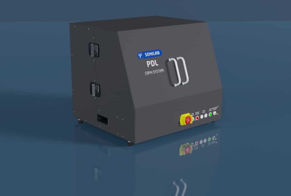
Building on work published in Nature by Oki Gunawan from IBM Research, the PDL-1000 system can differentiate between the Hall effect mobilities of holes and electrons in a material. This novel approach, called the Carrier Resolved Photo-Hall (CRPH) technique, unlocks information about cutting-edge materials that would otherwise require combining together several different characterization techniques. The CRPH technique has proven successful for studying a range of advanced materials, including perovskites, kesterites, thermoelectric compounds, transparent conducting oxides, organic semiconductors, as well as more traditional semiconductor materials.
In addition to the novel CRPH capability, the PDL-1000 can be equipped for mobility and carrier concentration measurements at cryogenic temperatures, opening up a new set of material characterization applications. This cryogenic option supports the full CRPH capability of the tool. The PDL-1000 system also supports both AC and DC Hall measurement modes, with the AC field measurement particularly useful for characterizing samples with low mobilities, including semiconductor, photovoltaic and thermoelectric materials.
The PDL-1000 is now commercially available and shipping to customers. To learn more, contact Semilab at info.usa@semilab.com.
- Visit Semilab at booth number #101

