Researchers in China have observed giant tunnelling magnetoresistance (TMR) in a magnetic tunnel junction made from the antiferromagnet CrSBr. When cooled to a temperature of 5 K, the new structure exhibited a magnetoresistance of 47,000% – higher than commercial magnetic tunnel junctions – and it retained 50% of this TMR at 130 K, which is well above the boiling point of liquid nitrogen. According to its developers, the structure can be manufactured in a way that is compatible with the magnetron sputtering process used to make conventional spintronics devices. These qualities, together with the fact that CrSBr is stable in air, make it a promising candidate platform for spintronic devices, they say.
Standard magnetic tunnel junctions (MTJs) consist of two ferromagnets separated by a non-magnetic barrier material. They are found in a host of spintronics technologies, including magnetic random-access memories, magnetic sensors and logic devices.
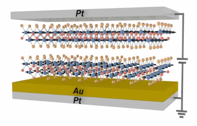
Junctions based on A-type van der Waals (vdW) antiferromagnets such as CrSBr and other chromium halides are an attractive alternative to conventional MTJs thanks to their unusually high tunnelling magnetoresistance. They work thanks to the spin-filter effect, in which the electron spins (or magnetic moments) of the chromium atoms in CrSBr are ferromagnetically coupled to other atoms in their layer and antiferromagnetically coupled to atoms in neighbouring layers. In other words, the spins align parallel to each other in the single layers and antiparallel to each other between neighbouring layers.
While the high tunnelling resistance of these so-called spin-filter MTJs (sf-MTJs) makes them good candidates for magnetic memories, they do have certain drawbacks. Notably, the materials they are made from tend to be unstable and prone to losing their magnetism at high temperatures. This makes it hard to use them in practical spintronic devices.
Overcoming fabrication challenges
In the latest study, researchers led by Guoqiang Yu of the Beijing National Laboratory for Condensed Matter Physics developed a new fabrication technique for these desirable materials. Working with colleagues in Beijing, Dongguan and Wuhan, they began by depositing a bilayer of platinum (Pt) and gold (Au) onto Si/SiO2 wafers using DC magnetron sputtering.
Next, members of the team mechanically shaved off thin flakes of CrSBr from a sample of the bulk material and placed them onto the Si/SiO2/Pt/Au substrates. This enabled them to obtain relatively thin CrSBr flakes on Pt/Au with clean and fresh surfaces. At this point, the researchers deposited a further layer of platinum onto the CrSBr with an ultralow sputtering power of 3–5 W and a relatively high deposition pressure of around 1 Pa. Finally, they used ultraviolet lithography and Ar ion milling to fabricate several sf-MTJs from the layered structure they created.
Promising properties
The new sf-MTJs have many favourable characteristics. “The first is that the route we employed to make them is more compatible with those employed to fabricate conventional spintronics metallic stacks,” Yu explains. “The second is that they retain 50% of their TMR even at a temperature of 130 K, which is so far the record-high working temperature for sf-MTJs.”
Yu points out that this record-high operating temperature is not far below CrSBr’s so-called Néel temperature, beyond which the material’s thermal energy prevents its spin moments from aligning. This relatively high operating temperature comes with an important practical advantage, Yu adds. “Compared to previous such junctions, our sf-MTJs might work in the liquid nitrogen temperature range and perhaps even at room temperature,” he observes. “And thanks to their stability in air, they are more suited to real-world applications.”

Large piezomagnetism appears in an antiferromagnet
That is not all. CrSBr is also a semiconductor, so its neighbouring layers have opposite magnetic moments at zero or small magnetic fields. This means it can be used as a barrier layer at low temperatures. “In this configuration, all the electrons, spin-up or spin-down, must encounter a higher barrier height after being polarized in one spin direction or another by passing through the first layer because the next layer has an opposite spin orientation, giving rise to higher tunnelling resistance,” Yu tells Physics World. “When the applied magnetic field is large enough, all the magnetic moments are aligned with this field and, in this case, the electrons with spins parallel to the field direction encounter a lower barrier height, which results in lower tunnelling resistance.”
The researchers, who report their work in Chinese Physics Letters, suggest that the new junctions could be used in spintronic devices based on a stack of a just a few layers of CrSBr. “Our study has revealed that sf-MTJs based on 2D vdW A-type antiferromagnets have some outstanding properties,” Yu says. “We will now be trying to find a 2D vdW A-type ferromagnet with a higher Néel temperature to further improve the working temperature of the junction we have made so that it is more suited to applications.”
A further challenge, the researchers say, will be to figure out a way to electrically manipulate the magnetization on the A-type antiferromagnet so they can construct fully functioning spintronic devices.
- SEO Powered Content & PR Distribution. Get Amplified Today.
- PlatoAiStream. Web3 Data Intelligence. Knowledge Amplified. Access Here.
- Minting the Future w Adryenn Ashley. Access Here.
- Buy and Sell Shares in PRE-IPO Companies with PREIPO®. Access Here.
- Source: https://physicsworld.com/a/giant-tunnelling-magnetoresistance-appears-in-an-antiferromagnet/
- :has
- :is
- :not
- 000
- 1
- 2D
- a
- above
- According
- Adds
- ADvantage
- After
- AIR
- align
- aligned
- All
- also
- alternative
- an
- and
- Another
- appears
- applications
- applied
- AR
- ARE
- around
- AS
- At
- attractive
- barrier
- based
- BE
- because
- began
- Beijing
- being
- below
- between
- Beyond
- by
- CAN
- candidate
- candidates
- case
- certain
- challenge
- characteristics
- China
- chromium
- colleagues
- comes
- commercial
- compatible
- Condensed matter
- Configuration
- construct
- conventional
- could
- coupled
- created
- dc
- deposited
- developed
- developers
- device
- Devices
- direction
- do
- drawbacks
- each
- effect
- electrons
- employed
- enabled
- energy
- enough
- Even
- Explains
- fact
- far
- few
- field
- Fields
- Figure
- Finally
- Find
- First
- For
- found
- fresh
- from
- fully
- functioning
- further
- giant
- Giving
- Gold
- good
- Hard
- Have
- he
- height
- High
- higher
- host
- http
- HTTPS
- image
- important
- improve
- in
- In other
- Including
- information
- issue
- IT
- ITS
- jpg
- just
- laboratory
- large
- latest
- layer
- layered
- layers
- Led
- Liquid
- logic
- losing
- Low
- lower
- made
- Magnetic field
- Magnetism
- make
- MAKES
- manufactured
- many
- material
- materials
- Matter
- max-width
- means
- Members
- Memories
- might
- Moments
- more
- must
- National
- New
- next
- notably
- now
- Observes
- obtain
- of
- off
- on
- ONE
- operating
- opposite
- or
- Other
- our
- out
- outstanding
- Parallel
- particularly
- Passing
- perhaps
- Physics
- platform
- platinum
- plato
- Plato Data Intelligence
- PlatoData
- Point
- points
- power
- Practical
- pressure
- prevents
- previous
- process
- promising
- properties
- qualities
- range
- real world
- relatively
- report
- researchers
- Resistance
- Results
- retain
- Revealed
- Rise
- Room
- Route
- say
- says
- Second
- semiconductor
- sensors
- several
- single
- small
- So
- so Far
- some
- Spin
- spins
- Stability
- stable
- stack
- Stacks
- structure
- Study
- such
- suggest
- team
- Technologies
- tells
- than
- Thanks
- that
- The
- their
- Them
- thermal
- These
- they
- this
- those
- Through
- thumbnail
- to
- together
- true
- two
- use
- used
- using
- W
- Way..
- we
- WELL
- when
- which
- WHO
- will
- with
- words
- Work
- working
- zephyrnet
- zero

