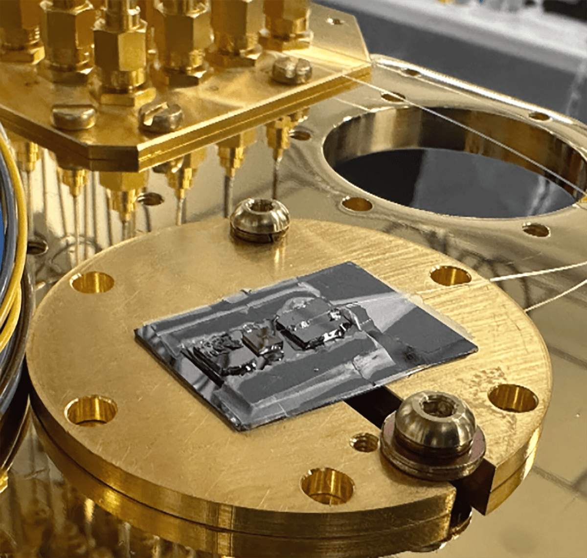
A research collaboration between Element Six and the AWS Center for Quantum Networking is harnessing the unique photonic and quantum properties of synthetic diamond to fashion the building blocks of long-distance quantum networks

While today’s fibre-optic networks distribute classical information across global length scales, the quantum networks of the not-so-distant tomorrow will exploit the exotic properties of entanglement and superposition to securely transmit quantum information between end-users at the same global scale. This capability will enable quantum-encrypted communications for all manner of organizations – from governments and banks to healthcare providers and the military – and open the way, inevitably, to the implementation of at-scale parallel quantum computing resources, with remote computing nodes linked quantum mechanically across the network.
Though still under development, quantum repeaters represent a core enabling technology as the quantum internet comes into view, serving a similar function as fibre amplifiers in classical optical networks by correcting for the loss and infidelity that occur as quantum information propagates over long distances (though without disrupting the quantum state of light as it passes through the network).
Quantum repeaters operate by transferring information encoded on photons onto a stationary memory qubit where the information can be stored and corrected. Defect qubits, such as colour centres in synthetic diamond, are shaping up as credible candidates for this task because they have an effective interface with light (the source of their colour) and because these defects can have a long-lived “spin” memory. Two classes of diamond-defect qubits are the focus of intense R&D interest in this regard: the nitrogen-vacancy spin centre (NV) and the silicon-vacancy spin centre (SiV), both of which are formed by removing two adjacent carbon atoms from a synthetic diamond crystal lattice and replacing them with a single nitrogen or silicon atom, respectively.

Here Bart Machielse, senior quantum research scientist at the AWS Center for Quantum Networking, tells Physics World how his team is accessing the leading-edge materials science and fabrication capabilities of research partner Element Six to realize “quantum advantage” in optical communications systems using synthetic diamond.
What’s the headline goal for the AWS quantum networking programme?
The AWS Center for Quantum Networking is located in Boston, Massachusetts, and has all the tools needed to support an independent R&D initiative in quantum communications. As such, we fabricate, test, characterize and optimize our own devices for proof-of-concept testing in long-distance quantum networking experiments. In my role, I lead the devices and packaging team with a remit to drive the scale-up and integration of quantum photonics (including synthetic diamond photonics) in high-grade research demonstrators of deployment-grade quantum networking technologies.
Presumably, collaboration is a given in such a competitive field?
It’s mandatory. We rely on R&D partners who can bring unique technical capabilities, deep domain knowledge and specialist know-how to the table. Our collaboration with Element Six, for example, is all about reimagining and transforming synthetic diamond as a material platform for photonic devices destined for applications in quantum memories and quantum repeaters. In brief, that means progressing from where we are now – a substrate that’s finnicky to work with when it comes to nanophotonic fabrication – to a material that’s compatible with scalable, reproducible and cost-effective semiconductor-style manufacturing.
How does the collaboration with Element Six work operationally?
Working with Element Six is a true R&D collaboration. For starters, there’s tight integration between the materials experts at Element Six and the quantum photonics team here at AWS. The collective conversation is key to successful translation of the baseline materials know-how at Element Six into enhanced device-level performance.
It’s all about the pipeline in this regard: our job at AWS is to take the diamond substrates that Element Six produces and apply our specialist optical, fabrication, microwave and cryogenic tools to better understand the quantum performance of that material when it’s being fabricated into photonic devices – in particular, how the optical emission maps versus fundamental materials properties such as dislocation density, strain, surface smoothness and the like.
What are the main manufacturing and engineering challenges when it comes to deploying synthetic diamond in quantum networking systems?
Right now, a lot of what we do in synthetic diamond photonics is highly probabilistic – for example, in terms of sample purity, the formation of defects, the exact location of those defects and the macro-scale crystal properties of the substrate material. In short, there is a lot of understanding needed to link the properties required for the application to the material specifications so that it can be fully scaled. In collaboration with Element Six, AWS is seeking to understand what the factors are that make synthetic diamond quantum-grade; also what the limits are when it comes to driving down the cost/complexity of materials processing so that you get what you need, not what you don’t need.

One thing is certain: Element Six’s commitment to ongoing investment in plasma-enhanced chemical vapour deposition (PECVD) growth techniques will be critical to the design, development and at-scale fabrication of diamond devices for quantum networking applications. The priorities are already clear: improving control over the types of defects created and the material incorporated during synthetic diamond growth; widening the different morphologies of diamonds that can be produced at scale; and simultaneously reducing the cost of manufacturing.
So put another way: materials innovation is nothing without control?
That’s correct. The task going forward is to remove all the variabilities from the synthetic diamond fabrication process so that we can optimize the design, integration and performance of quantum photonic devices and subsystems out in the network. Even more fundamental: when we fabricate a synthetic diamond photonic device today, we use the top few microns of a 0.5 mm thick diamond, so we need to find ways to be a lot more efficient. Think manufacturability, think cost reduction and, ultimately, synthetic diamond substrates that are more “fabbable” – i.e. compatible with standard semiconductor fabrication techniques.
What does the AWS technology roadmap look like in quantum networking?
In time, it should be possible to deploy, in volume, diamond photonic devices containing quantum memories that serve as quantum repeaters – essential building blocks for what we’re calling “entanglement distribution networks”. Near term, the R&D priority is to work with companies like Element Six to deliver the quantum-grade synthetic diamond substrates that will make the device-level engineering and systems integration more reliable, scalable and network-ready. Our hope is that advances in synthetic diamond fabrication will, sooner rather than later, yield downstream technology innovations that make AWS quantum communication systems a must-have tool in the network security and privacy arsenal of our corporate customers.
The search for a quantum ‘game-changer’
Quantum-grade synthetic diamond is being lined up for a whole new range of photonic applications in quantum computing, quantum metrology and quantum networking – many of which have no analogues in existing materials. The academic community, for its part, is focused on pushing the limits of what can be done with this material, leading to paradigm shifts in quantum performance, while industry is all about taking the current state-of-the-art and figuring out how best to package and integrate engineered synthetic diamond into next-generation quantum devices.
With translation from research lab to the market now front-and-centre, the measures of success for quantum diamond devices are increasingly defined along coordinates like reliability, robustness, manufacturability, scalability and cost/performance ratio. That shift in mindset and priority informs the work of the quantum development team at Element Six, which is applying its patented technology and know-how in PECVD fabrication to produce, at scale, quantum grades of single-crystal diamond containing controlled levels of NV and SiV spin centres for applications in quantum networking systems and beyond.

“Synthetic diamond can offer game-changing solutions and allow our customers and partners to do something that couldn’t be done before – from building a laser with unprecedented power densities to a synthetic diamond ‘acoustic dome’ with exceptionally high frequency characteristics,” explains Daniel Twitchen, chief technologist at Element Six.
“Bart Machielse and his team at AWS are a case in point,” he adds. “They came to us because, over the years, we have developed a large toolbox of synthetic diamond innovation capabilities. Our accumulated know-how aligns with the technical challenges that must be solved to realize a diamond quantum networking platform, plus we have demonstrated the ability to scale synthetic diamond into a production environment.”
At the same time, Element Six realizes that new growth markets for synthetic diamond will require solutions that make it easier for the material to be used – within the emerging quantum supply chain and elsewhere. “Ultimately, the need and opportunity lie not just in making quantum-grade synthetic diamond, but processing and integrating it within photonic devices,” notes Twitchen. “And, in so doing, reducing the barriers for adoption of synthetic diamond.”
Right now, the focus for Twitchen and his Element Six colleagues is to scale the company’s industrial partnerships in the field of quantum networking, having already established the potential of synthetic diamond in academic collaborations with leading quantum networking groups at TU Delft in the Netherlands as well as MIT and Harvard University in the US.
“What’s been missing to date,” concludes Twitchen, “is a big industry player saying it can roll out quantum communications systems by introducing a new generation of quantum-secure network services for their customers. They don’t come much bigger than AWS, so it’s exciting to be pooling our expertise in quantum-grade diamond with AWS’s know-how in photonics to make this vision a reality.”
- SEO Powered Content & PR Distribution. Get Amplified Today.
- PlatoData.Network Vertical Generative Ai. Empower Yourself. Access Here.
- PlatoAiStream. Web3 Intelligence. Knowledge Amplified. Access Here.
- PlatoESG. Carbon, CleanTech, Energy, Environment, Solar, Waste Management. Access Here.
- PlatoHealth. Biotech and Clinical Trials Intelligence. Access Here.
- Source: https://physicsworld.com/a/synthetic-diamond-how-materials-innovation-is-rewriting-the-rules-of-quantum-networking/
- :has
- :is
- :not
- :where
- $UP
- a
- ability
- About
- above
- academic
- accessing
- Accumulated
- across
- Adds
- adjacent
- Adoption
- advances
- Aligns
- All
- allow
- along
- already
- also
- Amazon
- an
- and
- Another
- Application
- applications
- Apply
- Applying
- ARE
- Arsenal
- AS
- Assembly
- At
- atom
- AWS
- Banks
- barriers
- Baseline
- BE
- because
- been
- before
- being
- BEST
- Better
- between
- Beyond
- Big
- bigger
- Blocks
- boston
- both
- bring
- Building
- built
- but
- by
- calling
- came
- CAN
- candidates
- capabilities
- capability
- carbon
- case
- Center
- centre
- centres
- certain
- chain
- challenges
- characteristics
- characterize
- chemical
- chief
- chip
- classes
- clear
- click
- collaboration
- collaborations
- colleagues
- Collective
- come
- comes
- commitment
- Communication
- communication systems
- Communications
- communications systems
- community
- Companies
- Company’s
- compatible
- competitive
- computing
- control
- controlled
- Conversation
- Core
- Corporate
- correct
- corrected
- Cost
- cost reduction
- cost-effective
- created
- credible
- critical
- Crystal
- Current
- Customers
- Daniel
- Date
- deep
- defined
- deliver
- demonstrated
- deploy
- deploying
- Design
- destined
- developed
- Development
- development team
- device
- Devices
- Diamond
- different
- dislocation
- distribute
- distribution
- do
- does
- doing
- domain
- done
- Dont
- down
- drive
- driving
- during
- e
- easier
- Effective
- efficient
- element
- elsewhere
- emerging
- emission
- enable
- enabling
- Engineering
- enhanced
- entanglement
- Environment
- essential
- established
- Even
- example
- exceptionally
- exciting
- existing
- Exotic
- experiments
- expertise
- experts
- Explains
- Exploit
- factors
- Fashion
- few
- field
- Find
- Focus
- focused
- For
- formation
- formed
- Forward
- Frequency
- from
- fully
- function
- fundamental
- generation
- get
- given
- Global
- global scale
- goal
- going
- Governments
- Group’s
- Growth
- Harnessing
- harvard
- Have
- having
- he
- headline
- healthcare
- here
- High
- highly
- his
- hope
- How
- HTTPS
- i
- image
- implementation
- improving
- in
- Including
- Incorporated
- increasingly
- independent
- industrial
- industry
- inevitably
- information
- informs
- Initiative
- Innovation
- innovations
- integrate
- Integrating
- integration
- interest
- Interface
- Internet
- into
- introducing
- investment
- issue
- IT
- ITS
- Job
- jpg
- just
- Key
- knowledge
- lab
- large
- laser
- later
- lead
- leading
- Length
- levels
- lie
- light
- like
- limits
- lined
- LINK
- linked
- located
- location
- Long
- Look
- look like
- loss
- Lot
- Main
- make
- Making
- mandatory
- manner
- manufacturing
- many
- Maps
- Market
- Markets
- massachusetts
- material
- materials
- max-width
- means
- measures
- Memories
- Memory
- Metrology
- Military
- Mindset
- missing
- MIT
- more
- more efficient
- much
- must
- Must-Have
- my
- Near
- Need
- needed
- Netherlands
- network
- Network Security
- networking
- networks
- New
- next-generation
- no
- nodes
- Notes
- nothing
- now
- NV
- of
- offer
- on
- ongoing
- onto
- open
- operate
- Opportunity
- Optimize
- or
- organizations
- our
- out
- over
- own
- package
- packaging
- paradigm
- Parallel
- part
- particular
- partner
- partners
- partnerships
- passes
- patented
- patented technology
- performance
- Photons
- Physics
- Physics World
- pipeline
- platform
- plato
- Plato Data Intelligence
- PlatoData
- player
- plus
- Point
- possible
- potential
- power
- priority
- privacy
- process
- processing
- produce
- Produced
- produces
- Production
- programme
- progressing
- properties
- prototype
- providers
- Pushing
- put
- Quantum
- quantum computing
- quantum information
- Quantum Internet
- quantum networking
- quantum networks
- quantum research
- Qubit
- qubits
- R&D
- range
- rather
- ratio
- Reality
- realize
- reducing
- reduction
- regard
- reliability
- reliable
- rely
- remote
- remove
- removing
- represent
- require
- required
- research
- Resources
- respectively
- rewriting
- roadmap
- robustness
- Role
- Roll
- rules
- same
- saying
- Scalability
- scalable
- Scale
- scale-up
- scales
- Science
- Scientist
- Search
- securely
- security
- seeking
- semiconductor
- senior
- serve
- Services
- serving
- shaping
- shift
- Shifts
- Short
- should
- Silicon
- similar
- simultaneously
- single
- SIX
- So
- Solutions
- something
- Source
- specialist
- specifications
- Spin
- Sponsored
- standard
- State
- state-of-the-art
- Still
- stored
- success
- successful
- such
- superposition
- supply
- supply chain
- support
- Surface
- synthetic
- Systems
- table
- Take
- taking
- Task
- team
- Technical
- techniques
- Technologies
- technologist
- Technology
- Technology Innovations
- tells
- term
- terms
- test
- Testing
- than
- that
- The
- the information
- the Netherlands
- The Source
- their
- Them
- There.
- These
- they
- thing
- think
- this
- those
- though?
- Through
- thumbnail
- time
- to
- today
- today’s
- tomorrow
- tool
- Toolbox
- tools
- top
- Transferring
- transforming
- Translation
- transmit
- true
- two
- types
- Ultimately
- under
- understand
- understanding
- unique
- unprecedented
- us
- use
- used
- uses
- using
- Versus
- View
- vision
- volume
- Way..
- ways
- we
- WELL
- What
- when
- which
- while
- WHO
- whole
- will
- with
- within
- without
- Work
- world
- years
- Yield
- You
- zephyrnet


