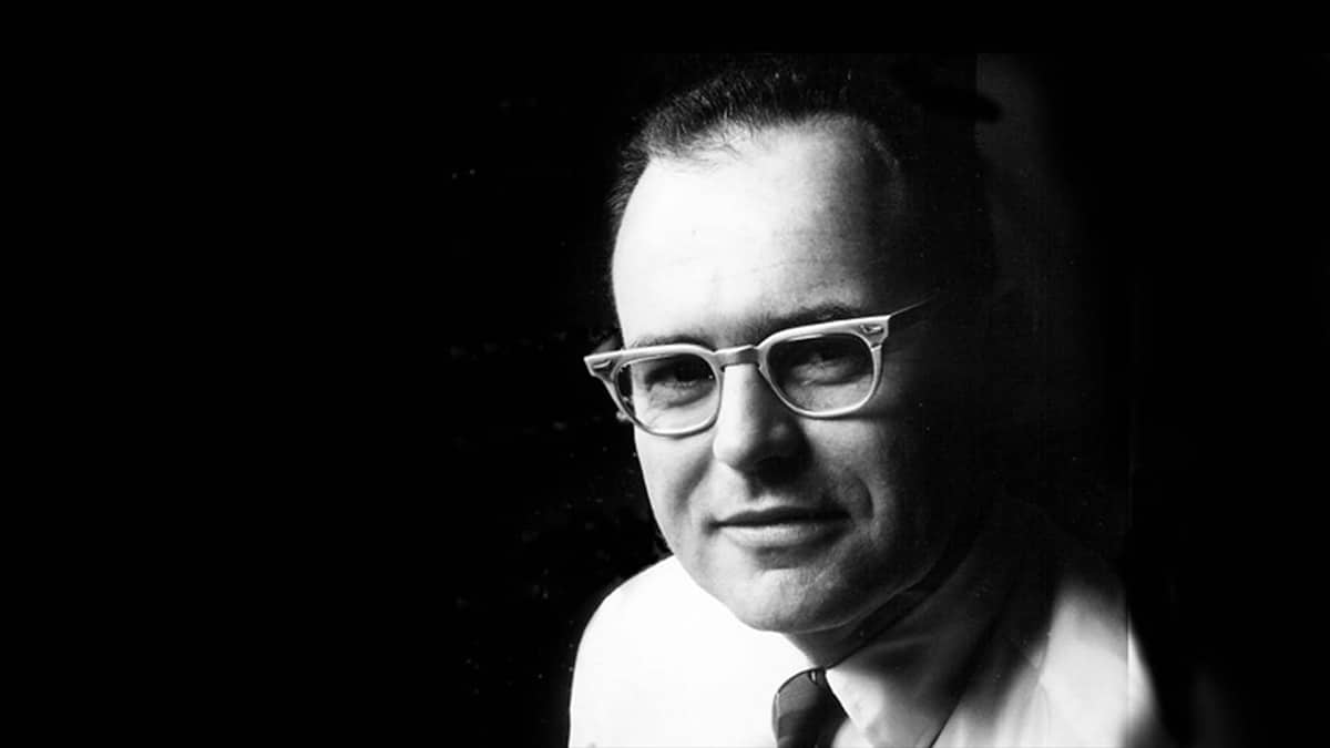
Gordon Moore, the co-founder of Intel who died earlier this year, is famous for forecasting a continuous rise in the density of transistors that we can pack onto semiconductor chips. James McKenzie looks at how “Moore’s law” is still going strong after almost six decades, but warns that further progress is becoming harder and ever more expensive to sustain
When the Taiwan Semiconductor Manufacturing Company (TSMC) announced last year that it was planning to build a new factory to produce integrated circuits, it wasn’t just the eye-watering $33bn price tag that caught my eye. What also struck me is that the plant, which is set to open in 2025 in the city of Hsinchu, will make the world’s first “2 nanometre” chips. Smaller, faster and up to 30% more efficient than any microchip that has come before, TSMC’s chips will be sold to the likes of Apple – the company’s biggest customer – powering everything from smartphones to laptops.
But our ability to build such tiny, powerful chips shouldn’t surprise us. After all, the engineer Gordon Moore – who died on 24 March this year, aged 94 – famously predicted back in 1965 that the number of transistors we can squeeze onto an integrated circuit ought to double every year. Writing for the magazine Electronics (38 114), Moore reckoned that by 1975 it should be possible to fit a quarter of a million components on to a single silicon chip with an area of one square inch (6.25 cm2).
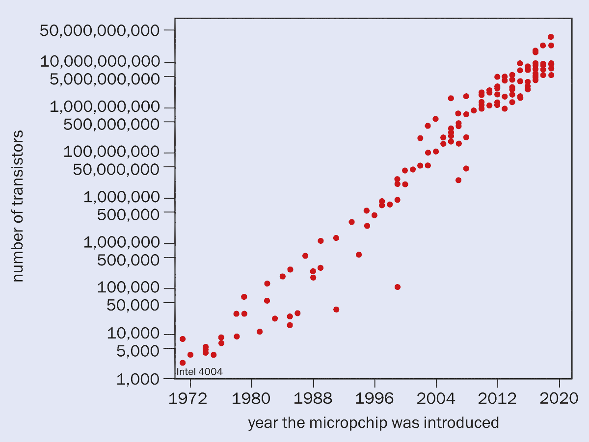
Moore’s prediction, which he later said was simply a “wild extrapolation”, held true, although in 1975 he revised his forecast, predicting that chip densities would double every two years, rather than every year. What thereafter became known as “Moore’s law” proved amazingly accurate, as the ability to pack ever more transistors into a tiny space underpinned the almost non-stop growth of the consumer electronics industry. In truth, it was never an established scientific “law” but more a description of how things had developed in the past as well as a roadmap that the semiconductor industry imposed on itself, driving future development.
Seeing into the future
Basic physics says that as transistors get smaller, they can be run faster and require less power. Simple economics, meanwhile, dictates that as you pack more transistors onto a chip, each transistor becomes cheaper to make. “The cost per component,” Moore noted in his 1965 article, “is nearly inversely proportional to the number of components.” A research director at the US firm Fairchild Semiconductor at the time, Moore simply put the two notions together.
Gordon Moore proved to be a visionary who correctly foresaw the breath-taking pace at which semiconductor technology would grow
In doing so, Moore proved to be a visionary who correctly foresaw the breath-taking pace at which semiconductor technology would grow. While the precise details of how we have shrunk transistors have changed over the years, many of Moore’s predictions about the rise of integrated circuits have come to pass. In his original article, he foresaw digital watches, home computers, smartphones (or what he called “personal portable communications equipment”), the ability to send multiple messages down phone lines, as well as automatic controls for cars.
In an interview with IEEE Spectrum on the 50th anniversary of his 1965 article, Moore said he was surprised that his law had survived for so long. “I never would have anticipated anyone remembering it this far down the road,” he said. Its continuation was, for him, a tribute to the creativity of engineers in the semiconductor industry, who have time and again found new ways to shrink devices. “I could never see more than the next couple of [chip] generations, and after that it looked like [we’d] hit some kind of wall. But those walls keep receding.”
However, in the same interview, Moore recognized that there are two basic physical obstacles that will eventually preclude any further miniaturization. As he recalled the cosmologist Stephen Hawking once pointing out on a visit to Silicon Valley, nothing can travel faster than the speed of light, while materials are, ultimately, made of atoms of a finite size. There are, in other words, speed and size limits to chips. “These are fundamentals I don’t see how we [will] ever get around,” Moore warned. “And in the next couple of generations, we’re right up against them.”
So is the end of Moore’s law in sight?
Gordon Moore: a brief history
Born on 3 January 1929 in Pescadero, California, Gordon Earle Moore was a chemist by training, graduating in 1950 from the University of California, Berkeley. He then did a PhD, also in chemistry, at the California Institute of Technology followed by a postdoc at the Applied Physics Laboratory at Johns Hopkins University from 1953 to 1956. That year he left academia to work at the Shockley Semiconductor Laboratory (SSL), which had just been set up by the physicist William Shockley.
It was an exciting time for the nascent semiconductor industry. SSL was one of the first high-tech firms in Silicon Valley to work on semiconductor devices and Shockley himself was awarded the 1956 Nobel Prize for Physics – along with Walter Brattain and John Bardeen – for their discovery of transistors. Moore was part of a group of talented young scientists whom Shockley recruited to develop and produce new semiconductor devices.
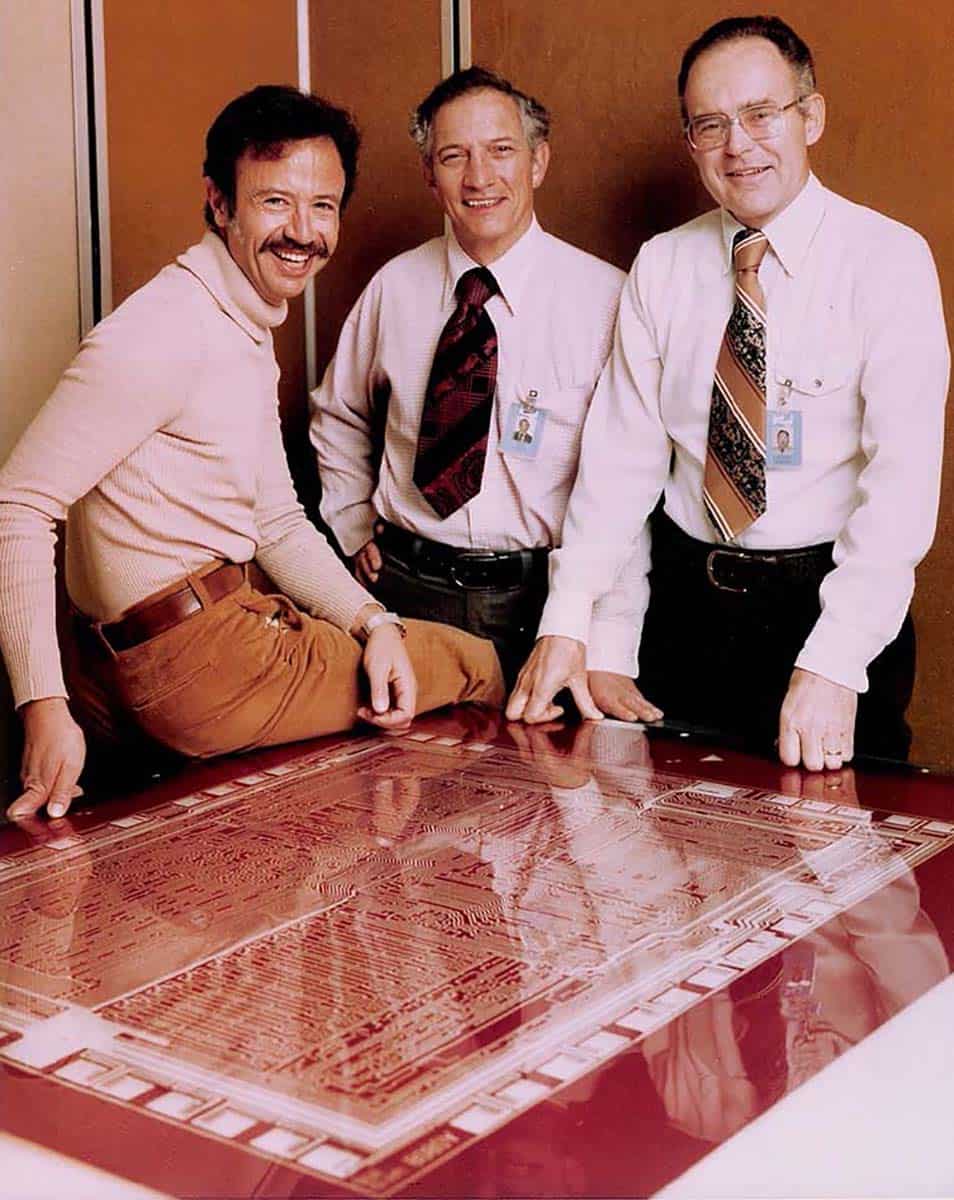
However, Shockley was not an easy boss to work for, with an authoritarian management style. After a demand for him to be replaced was rebuffed, Moore and other colleagues quit in 1957. Later known as the “traitorous eight”, they immediately founded their own company – Fairchild Semiconductor – with Shockley calling their departure a “betrayal”. The firm was named after Sherman Fairchild, an experienced business executive who invested in the company. It was while working as research director at Fairchild in 1965 that Moore made his famous prediction later dubbed “Moore’s law”.
Fairchild Semiconductor soon grew into a leader in the semiconductor industry, being bought by ON Semiconductor for $2.4bn in 2016. Operating as an incubator for new technology, it was directly or indirectly involved in the creation of dozens of corporations, including Intel and AMD. According to an analysis by Endeavor Insight in 2014, a total of 92 publicly listed firms, with a market value of more than $2.1 trillion, were spawned directly or indirectly by Fairchild. Endeavor reckoned that a further 2000 firms could be traced back to Fairchild too.
Perhaps the most famous of all is Intel, which was set up in 1968 by Moore and the physicist Bob Noyce, a fellow co-founder of Fairchild. Originally known by their initials as NM Electronics, it was soon renamed Intel, and Moore went on to hold various senior roles, including chairman and chief executive. Intel, which pioneered new technologies for computer memory, integrated circuits and microprocessor design, had revenues of $63bn in 2022 and employs more than 125,000 staff.
At his death, Moore was reportedly worth $7bn but he was a prolific philanthropist, setting up the Gordon and Betty Moore Foundation in 2000 with a $5bn gift to support educational and environmental projects. The following year he gave Caltech $600m, which was then the biggest gift to a higher-education institution. Moore also received many honours, including the Presidential Medal of Freedom (America’s highest civilian award) from George Bush in 2002.
Smaller, faster, better
At the heart of any computer is the central processing unit or CPU, which consists of individual transistors linked together to form a single integrated circuit that carries out basic arithmetical operations. The world’s first single-chip microprocessor was the four-bit CPU released by Intel in 1971. Known as the Intel 4004, it had 2300 transistors, each about 10 µm in size and sold for $60. But as Moore predicted, the number of transistors on integrated circuits would quickly rise.
By the early 1980s, transistors were down to 1 µm in size and companies were packing up to 100,000 transistors onto a chip. The number of transistors per chip reached a million by the 1990s, 10 million by the early 2000s and 100 million a decade later. The latest CPUs have over 10 billion transistors using what’s known as a “5 nm process”, with Intel managing to pack over 100 million transistors on each square millimetre by 2019. (These days the process name is essentially a marketing term: the 2 nm of TSMC’s chips, for example, doesn’t actually refer to any specific physical feature on the devices.)
Modern integrated circuits are created by taking a substrate of silicon or some other semiconductor, and then gradually building the circuit up layer by layer using various “lithographic” techniques. There is a huge variety of such methods, but all generally involve using either light or chemical reactions. What’s amazing is not just the incredible progress achieved in making chips, but also the sheer levels of cleanliness that are required in today’s semiconductor fabrication plants.
Back in 1971, the Intel 4004 chip was made using a “10 µm process”, which then meant that all transistors on the chips were spaced no more than 10 µm apart. To achieve such small dimensions, Intel pioneered the use of the “optical mask” – essentially a large, transparent glass plate, parts of which were covered with a pattern of light-absorbing chrome. Blue light was shone through the mask, which was held above the surface of the wafer.
Intel’s clever thinking was to coat the wafer with a light-sensitive organic photoresistive layer, which reacts if light lands on it, while areas that are unexposed stay the same. Using a solvent to dissolve away the parts that had been exposed to light, the original pattern on the mask could then be transferred to the silicon, albeit now much smaller (see image). Several masks steps were used to form the devices needed in the integrated circuit.

Over the years, increasingly accurate “projection lenses” had to be introduced between the mask and the wafer to make circuits smaller. In the 1980s, for example, “reduction steppers” were developed to make 2 µm chips. These devices transferred the mask patterns in stages to smaller and smaller lengths. Steppers continued to dominate lithographic patterning throughout the 1990s, as minimum feature sizes reached the 250 nm levels.
Ultimately, however, the smallest feature you can print is limited by two factors: the resolving capability of the photoresist and the minimum size of the image that can be projected onto the wafer. That minimum size – also known as the Rayleigh criterion or the “diffraction limit” – is given by 0.61 λ/NA, where λ is the wavelength of light and NA is the numerical aperture of the projection lens. In other words, it’s impossible to project the image of a feature less than roughly half the wavelength of the light being used.
To get to ever-smaller sizes, lithography systems over the years shifted to ever-shorter wavelengths, progressing from blue (436 nm) to ultraviolet (365 nm) and then to deep ultraviolet light (248 nm), with the latest systems using 193 nm light from an argon fluorine excimer laser. Moore’s law has also been sustained by improvements in numerical apertures, which have been pushed from 0.16 in early systems to amazingly high values of up to 0.93. Huge advances in nano-positioning technology to align the various masks to a suitable accuracy have been vital too.
Down to 2 nm
But how do we get to the 2 nm process as used at plants like that of TSMC in Taiwan? That’s well below the diffraction limit even for light with an ultra-short wavelength of 193 nm. Most chip manufacturers have turned to systems developed by the Dutch multinational firm ASML. Using extreme ultraviolet (EUV) light with a wavelength of 13.5 nm, which is almost in the X-ray range, these devices are incredible feats of engineering that push hard on the boundaries of the laws of physics.
The EUV light is created by blasting molten drops of tin with a laser in a vacuum and then bouncing it off mirrors made by Zeiss, which ASML says are the flattest surfaces in the world. Costing more than $150m a pop, each ASML system is huge, having to be shipped to customers in 40 massive freight containers, three cargo planes and more than 20 trucks. Despite the price, the company has so far sold more than 140 of these EUV systems. But as the only supplier, ASML is in fact a bottle neck for expansion of the semiconductor industry.
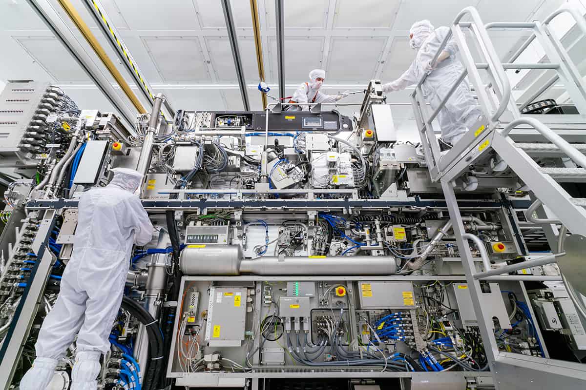
According to MIT Technology Review, the first generations of chips with tiny EUV features are already being used by Google and Amazon, improving language translation, search-engine results, photo recognition and AI. The EUV revolution is also reaching everyday consumers, with ASML’s machines being used to make chips in smartphones from the likes of Apple and Samsung.
Also helping us to keep Moore’s law going are some amazing advances in materials science and transistor design. Take, for example, “fin field-effect transistors” or FinFETS, which use relatively tall, fin-like structures on the surface of the silicon base. FinFETS were among the first of a new generation of 3D transistors that can be stacked one on top of the other. Companies are already producing devices with 176 mask layers, but 600 layers and above are on the semiconductor industries’ roadmap to deliver future generations of devices.
The latest 2 nm processes use even more advanced FET transistors, known as gate all around (GAA) devices. The US firm IBM has already used them to create chips with a density of 333 million transistors per square millimetre, with the company claiming it can fit 50 billion transistors “onto a chip the size of a fingernail”. IBM says such chips could quadruple smartphone battery life, cut the cost of data centres and make laptops run faster.
Working at the limit
Essentially what is happening is that every possible lever is being pulled to keep Moore’s law on track. ASML, for example, is working towards the 1 nm chip scale using EUV lithography systems, while we can expect to see further improvements in lithography, with the resolution usually halving every six years. It is worth the effort: processors made with TSMC’s 2 nm silicon chips, for example, will run up to 15% faster than with 3 nm devices, while consuming about 25% less energy.
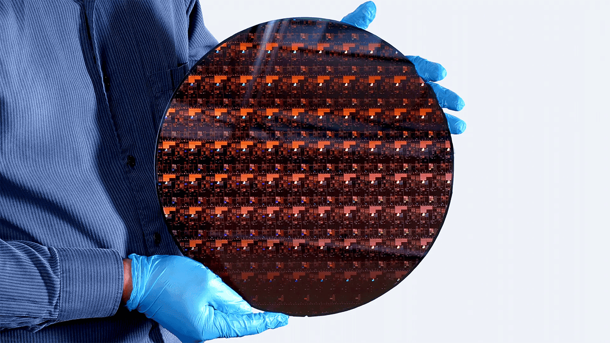
We are certainly not yet done with Moore’s law. Although 2 nm is barely the width of 10 silicon atoms, remember the transistors in 2 nm chips aren’t actually that small; the distance from one gate to another is nearer to 50 nm (the so-called “gate pitch”) so there is a bit more room to play with. We can also wring more out of existing chips by writing software code that is more efficient.
But it is hard to see what innovations will come next to keep Moore’s law going. In 2016 researchers in Germany, Japan and the US made a transistor consisting of one molecule of phthalocyanine surrounded by just 12 indium atoms, which – with a gate size of 0.167 nm – would be “the absolute hard limit for Moore’s law” (Nat. Phys. 11 640). There is also a move to different kinds of chips designed for specific applications, such as AI, which use graphical processing units (GPUs) rather than CPUs and so can calculate more effectively in parallel.
In the end, how far we can stretch Moore’s law is likely to be a matter of pure economics. With TSMC’s newest factory costing $33bn – far more than the $15—20bn of 5 nm plants – sustaining Moore’s law is a game of very high stakes. In this rarefied atmosphere, only a handful of players – IBM, Intel, Samsung and TSMC – are capable of developing next-generation semiconductor chip technology. They certainly haven’t given up on Moore’s law, but further progress is going to be very hard to sustain.
- SEO Powered Content & PR Distribution. Get Amplified Today.
- EVM Finance. Unified Interface for Decentralized Finance. Access Here.
- Quantum Media Group. IR/PR Amplified. Access Here.
- PlatoAiStream. Web3 Data Intelligence. Knowledge Amplified. Access Here.
- Source: https://physicsworld.com/a/moores-law-further-progress-will-push-hard-on-the-boundaries-of-physics-and-economics/
- :has
- :is
- :not
- $10 million
- $UP
- 000
- 1
- 10
- 100
- 12
- 13
- 15%
- 16
- 1998
- 20
- 2016
- 2019
- 2022
- 2023
- 2025
- 24
- 25
- 250
- 3d
- 40
- 50
- a
- ability
- About
- above
- Absolute
- Academia
- According
- accuracy
- accurate
- Achieve
- achieved
- actually
- advanced
- advances
- After
- again
- against
- aged
- AI
- align
- All
- along
- already
- also
- Although
- amazing
- Amazon
- AMD
- among
- an
- analysis
- and
- Andrew
- Anniversary
- announced
- Another
- Anticipated
- any
- anyone
- apart
- Apple
- applications
- applied
- Applying
- Archive
- ARE
- AREA
- areas
- around
- article
- AS
- At
- Atmosphere
- Authoritarian
- Automatic
- award
- awarded
- away
- back
- base
- basic
- battery
- Battery life
- BE
- became
- becomes
- been
- before
- being
- below
- Berkeley
- between
- Biggest
- Billion
- Bit
- Blue
- board
- BOSS
- bought
- boundaries
- build
- Building
- business
- but
- by
- calculate
- california
- called
- calling
- CAN
- capability
- capable
- cars
- caught
- central
- centre
- centres
- certainly
- chairman
- changed
- cheaper
- chemical
- chemistry
- chief
- chip
- Chips
- Chrome
- City
- click
- Co-founder
- co-founders
- code
- coined
- colleagues
- COM
- come
- Communications
- Companies
- company
- Company’s
- component
- components
- computer
- computers
- Consisting
- consists
- consumer
- Consumers
- Containers
- continuation
- continued
- continuing
- continuous
- controls
- CORPORATION
- Corporations
- Cost
- could
- Couple
- covered
- covering
- create
- created
- creation
- creativity
- customer
- Customers
- Cut
- Dark
- data
- data centres
- Days
- decade
- decades
- deep
- deliver
- Demand
- description
- Design
- designed
- Despite
- details
- develop
- developed
- Developer
- developing
- Development
- Devices
- dictates
- DID
- died
- different
- digital
- dimensions
- directly
- Director
- discovery
- distance
- do
- Doesn’t
- doing
- Dominate
- done
- Dont
- double
- down
- dozens
- driving
- Drops
- dubbed
- Dutch
- each
- Earlier
- Early
- easy
- Economics
- educational
- effectively
- efficient
- effort
- either
- Electronics
- employs
- end
- endeavor
- ends
- energy
- engineer
- Engineering
- Engineers
- environmental
- equipment
- essentially
- established
- Even
- eventually
- EVER
- Every
- everyday
- everything
- example
- exciting
- executive
- existing
- expansion
- expect
- expensive
- experienced
- Explain
- exposed
- extreme
- eye
- fabricating
- fact
- factors
- factory
- famous
- famously
- far
- faster
- Feature
- Features
- fellow
- FET
- Firm
- firms
- First
- fit
- followed
- following
- For
- Forecast
- form
- found
- Founded
- from
- Fundamentals
- further
- future
- game
- generally
- generation
- generations
- George
- Germany
- get
- getting
- gift
- given
- glass
- going
- GPUs
- gradually
- graph
- Group
- Grow
- grown
- Growth
- had
- Half
- Halving
- handful
- Happening
- Hard
- Have
- having
- he
- Heart
- Held
- helping
- High
- highest
- him
- his
- Hit
- hold
- Home
- How
- However
- HTML
- http
- HTTPS
- huge
- i
- IBM
- IEEE
- if
- image
- immediately
- imposed
- impossible
- improvements
- improving
- in
- In other
- Including
- increasingly
- incredible
- incubator
- indirectly
- individual
- industry
- information
- innovations
- inside
- insight
- Institute
- Institution
- integrated
- Intel
- Interview
- into
- introduced
- invested
- involved
- issue
- IT
- ITS
- itself
- January
- Japan
- Johns Hopkins University
- jpg
- just
- Keep
- Kind
- known
- laboratory
- lands
- language
- laptops
- large
- laser
- Last
- Last Year
- later
- latest
- Law
- Laws
- layer
- layers
- leader
- left
- less
- levels
- Life
- light
- like
- likely
- likes
- LIMIT
- Limited
- limits
- lines
- linked
- Listed
- Long
- looked
- LOOKS
- Machines
- made
- magazine
- make
- MAKES
- Making
- management
- managing
- Manufacturers
- manufacturing
- many
- March
- Market
- market value
- Marketing
- mask
- Masks
- massive
- materials
- Matter
- max
- max-width
- me
- meant
- Meanwhile
- Memory
- messages
- methods
- million
- minimum
- molecule
- more
- more efficient
- most
- move
- much
- multinational
- multiple
- my
- name
- Named
- nascent
- Nature
- nearly
- needed
- never
- New
- New technologies
- Newest
- next
- next-generation
- no
- nobel prize
- noted
- nothing
- now
- number
- obstacles
- of
- off
- on
- once
- ONE
- only
- open
- operating
- Operations
- or
- organic
- original
- originally
- Other
- our
- out
- over
- own
- Pace
- Pack
- Parallel
- part
- particular
- parts
- pass
- past
- Pattern
- patterns
- phone
- photo
- photo recognition
- physical
- Physics
- Physics World
- pioneered
- Plants
- plato
- Plato Data Intelligence
- PlatoData
- Play
- players
- pop
- possible
- power
- powerful
- Powering
- precise
- predicted
- predicting
- prediction
- Predictions
- price
- prize
- process
- processes
- processing
- processors
- produce
- Produced
- Progress
- progressing
- project
- projected
- Projection
- projects
- proved
- publicly
- publicly listed
- Push
- pushed
- put
- Quarter
- quickly
- range
- Rate
- rather
- reached
- reaching
- React
- reactions
- Reacts
- received
- recognition
- recognized
- relatively
- released
- remain
- remember
- remembering
- replaced
- require
- required
- research
- researchers
- Resolution
- resolving
- Results
- revenues
- Revolution
- right
- Rise
- road
- roadmap
- ROBERT
- roles
- Room
- roughly
- Run
- s
- Said
- same
- Samsung
- says
- Scale
- Science
- scientific
- scientists
- see
- semiconductor
- semiconductor chip
- send
- senior
- set
- setting
- several
- Sherman
- shifted
- shipped
- should
- Shows
- Sight
- Silicon
- Silicon Valley
- Simple
- simply
- since
- single
- SIX
- Size
- sizes
- small
- smaller
- smartphone
- smartphones
- So
- so Far
- Software
- sold
- some
- soon
- Space
- specific
- speed
- square
- Squeeze
- SSL
- stacked
- Staff
- stages
- stay
- Stephen
- Steps
- Still
- strong
- style
- such
- suitable
- support
- Surface
- surprise
- surprised
- surrounded
- Survived
- system
- Systems
- TAG
- Taiwan
- Take
- taking
- talented
- techniques
- Technologies
- Technology
- term
- than
- that
- The
- the world
- their
- Them
- then
- There.
- These
- they
- things
- thinker
- Thinking
- Third
- this
- this year
- those
- three
- Through
- throughout
- thumbnail
- time
- to
- today’s
- together
- too
- top
- Total
- towards
- track
- Training
- transferred
- Translation
- transparent
- travel
- Trend
- Trillion
- Trucks
- true
- truth
- Tsmc
- Turned
- two
- Ultimately
- underpinned
- unit
- units
- university
- University of California
- us
- use
- used
- using
- usually
- Vacuum
- Valley
- value
- Values
- variety
- various
- very
- visionary
- Visit
- vital
- Wall
- Warns
- was
- watches
- ways
- we
- WELL
- went
- were
- What
- What is
- when
- which
- while
- WHO
- width
- Wikipedia
- will
- with
- words
- Work
- working
- world
- world’s
- worth
- would
- writing
- x-ray
- year
- years
- yet
- You
- young
- zephyrnet


